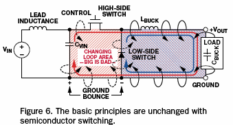
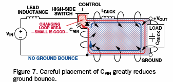
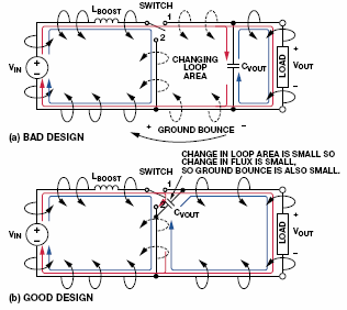
The following diagrams are taken from:
http://www.analog.com/library/analogdialogue/archives/41-06/ground_bounce.html
Buck DCDC Converters
This is bad:
This is good:
Boost DCDC Converters
Ground Bounce Design Tips
Switcher IC’s with internal mosfets tend to aim towards higher efficiency and therefore lower mosfet on resistance. However low on resistance means faster switching times, which contributes to noise and ground bounce. Should you consider a less efficient IC with a higher on resistance? You can’t easily add resistance externally as the resistance your aiming for is still very low (e.g. 100 or more milli Ohms).
For a boost design get the output capacitor cathode right next to the switchers mosfet ground pin. A few extra mm of tracking can cause issues on some designs. Keep the inductor to diode and diode to capacitor tracking very short.
Can you shut-down the DCDC converter while doing sensitive measurements? If your doing periodic fast AtoD readings then whilst not an ideal solution, including the means to shut-down the DCDC converter whilst the AtoD is sampling can be a compromise solution in suitable applications.
High Current Design Tips
If changing layers for any of the tracking, including the power supply to the switcher, vias can create significant resistance so use multiple vias to remove this issue.
Boost designs where the load can draw high currents can be very problematic. Often the source is batteries where the voltage will drop as the load appears, or for low input voltages the power supply may need to be supplying high currents. Once you build your prototype you may find that the say 3.0V to 5V @ 3A switch mode design which the switcher IC data sheet says will work just fine actually doesn’t. So when designing these types of boost switch mode circuits you may want to consider:
Can you use multiple switch mode circuits to supply different loads, so that the power each has to output is reduced? Often a problem switcher design will work fine if the load current is reduced.
Can you use a switchmode IC with an adjustable switching frequency? If possible use one as it gives you an important parameter to adjust when trying to solve a problem.
Can you use 2oz copper on the PCB to reduce the resistance of power supply tracks?
Reduce the length of power input tracks. If there is a risk that when you come to test your design it fails until you directly wire the power source to the inductor and mosfet consider this now and reduce the the track lengths the power input takes to get there and increase their copper width. This is a classic problem!
Is there a chance you’ll need to increase input or output capacitance for the switcher – if you can add the footprints at the design stage just in case. Remember that low ESR is often more important than capacitor size for switchmode supplies.
Could the tracking be improved in any way? If so do it now instead of finding out the hard way! If the switcher IC data sheet includes a recommended PCB layout does your layout match? Could it? Their layout works so if you can match it your chances of success are increased.
Read the switcher data sheet in it’s entirety. Often there are hidden away mentions of additions to the recommended circuit useful in specific applications which may apply to your circuit.
Does the IC have an evaluation board? If so read it’s data sheet to check if there is anything helpful in it you haven’t considered.
Solving Ground Bounce Problems
The primary cause of ground bounce is poor PCB design, or more typically non optimal PCB design. These notes refer to boost switcher, but apply for a buck switcher also by adjusting for the different wiring arrangement.
A classic method to solving it is to start adding or changing capacitors, but this usually only has a very limited effect.
A good starting point to identifying the problem and curing it is to start by removing as many imperfections as possible:
Power the PCB with 0Vin connected directly to the switchers GND point, and with +Vin connected near to the inductor.
If the main capacitor is not connected ideally as above lift it and make it perfect using short wire links if necessary.
These two steps will give you a good starting point. Has the ground bounce reduced or gone away?
Scope from the switchers GND point (mosfet ground) to the +V terminal of the main capacitor. Is there noise? There may be only a very short link but if you have noise between these two points then maybe you have the cause of your problem? It might seem impossible for there to be noise from an inch of copper or wire, but it isn’t and if it’s there you need to eradicate it.
Check there isn’t an area elsewhere in the circuit causing or contributing to the noise by powering the PCB after the switcher (i.e. at its output so it’s no longer used). Is the supply to the rest of the circuit now perfectly clean?
With the switcher powered again use a scope with its GND connected to the switchers GND point (DCDC converter IC power ground or external mosfet ground) and probe different areas of the PCB. Does the noise level change depending on where you probe? Probe to other GND points also. If so this is likely to indicate areas of the circuit contributing to the noise. What is the GND connection to that area like? Does the noise reduce if you provide it with a direct dedicated GND connection to the switchers GND point?
Multilayer PCB 0V ground planes are great at reducing signal noise around a circuit, but are not necessarily great at reducing switcher ground bounce issues (as with audio they can often be a cause of new problems). Should your power circuitry use a separate GND to the GND power plane or should the ground plane include some cuts to direct the switcher current? Don’t assume because there is a great big ground plane connecting to an area of the PCB that it’s therefore got a perfect GND connection. Remember that true ground will be at one point of the PCB (i.e. at the 0V power connection in or at the GND connection of the switcher). All other points returning current are not grounds but just return lines to ground.
Are there big capacitors elsewhere on the PCB that are affecting the switchers main capacitor being able to provide the perfect switch mode supply arrangement? Are they part of the current path during switching? Ensure the main capacitor is a low ESR (low impedance) type.
Does changing the switchers diode to a different part help? It often shouldn’t but we’ve occasionally found that using a totally different model can sudenly cure much of a noise problem so it’s worth trying in case. Remember that diode switching times are often only specified as a maximum value, not a typical. Slower diodes can sometimes help.
Have a beer, then come back and read the switcher IC datasheet for a 10th time. Hidden in the horrible technical detail may be something you’ve overlooked or that sparks a new process of elimination. Get a piece of paper and draw out how you think the current is flowing in PCB traces. Does that match the actual tracking and physical layout of the PCB?
Remember, the theory is sound but any PCB layout isn’t perfect. The problem is being caused by something that isn’t perfect enough – you just need to work through every detail and find it. If your new to switch mode design don’t worry, even experienced experts still get bitten by this stuff once in a while and the best way to learn the pitfalls is to find your way out of them – you only have to learn a mistake once.
More extreme solutions:
Should you completely isolate a sensitive area or the non high power area of the circuit? Can you use a separate mains transformer winding or an isolated DCDC converter to power the other section of the circuit? If you can this is often be a great solution. You can then choose the one perfect point to connect the isolated GND rails. Alternatively for more extreme issues should they remain isolated with opto isolated signals between them?
Ground Bounce Resources
You can never get your hands on enough ideas about solving ground bounce when faced with it!
http://www.analog.com/library/analogdialogue/archives/41-06/ground_bounce.html
http://homepages.which.net/~paul.hills/Emc/BecBody.html
http://www.edn.com/article/466994-Reducing_ground_bounce_in_dc_dc_converter_applications.php


