Basic MOSFET Selection Rules / Checks
The Drain to Source max voltage rating (max Vds) determines the maximum voltage you can switch.
The Gate threshold voltage determines the voltage difference you need to apply to the gate to make the mosfet conduct.
The Gate to Source max voltage (max Vgs) is a critical factor that must not be exceeded (even for a few nS) or the MOSFET can be destroyed. Will the power rails spike? If so provide protection of some sort (e.g. transient suppressor) or select a device with a higher rating. When switching high voltage rails (e.g. 24V from low voltage logic you can often meet this requirement using a potential divider to provide the mosfet with a gate voltage above 0V.
Do you need to use a mosfet driver IC? If the mosfet has a high Gate switching current (e.g. high current MOSFETs) or will be switched fast (to ensure that the mosfet operates efficiently with minimal power dissipation) then this may be necessary.
Check the ‘Why MOSFETs Fail’ notes below
General Notes
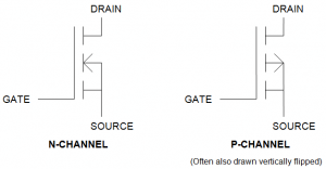
Enhanced MOSFETs when on allow current in either direction with an essentially identical RDSON. When off they block current in one direction.
Because of their high input impedance MOSFET’s are vulnerable to damage by electrostatic discharges. Sometimes they have integral protection diodes or zeners.
Enhancement mode mosfets incorporate a diode between the source and drain pins.
A double enhanced mosfet incorporates two diodes cathode to cathode.
A MOSFET only requires gate current during the switching edge, to charge the GS capacitance. This gate current can be high.
To Switch 0V
Use a N-Channel MOSFET with Source connected to 0V (either directly or via a current limiting resistor) and the load connected to Drain.
Whenever the Gate voltage exceeds the Source voltage by at least the Gate Threshold Voltage the MOSFET conducts. The higher the voltage, the more the Mosfet can conduct.
N channel mosfets have lower on resistances than P channel mosfets so are preferable if you have the choice of which side to switch.
N-Channel MOSFETs can also switch +V in certain configurations, with Drain being Vin and Source being switched Vout.
To Switch +V With A P-Channel MOSFET
Use a P-Channel MOSFET with Source connected to +V (either directly or via a current limiting resistor) and the load connected to Drain.
Usually the Source pin must be more positive than the Drain (however this isn’t true when using a P Mosfet to provide reverse polarity protection for instance).
Whenever the Gate voltage is lower than the (Source Voltage – Gate Threshold voltage) the MOSFET conducts. If the gate voltage is higher than this it does not conduct. The greater the voltage difference from the Source the more the MOSFET can conduct.
P channel mosfets have higher on resistances than N channel mosfets so are often less preferable.
The P-channel MOSFET has an advantage over the N-channel MOSFET for some applications due to the simplicity of the on/off control. A N-channel mosfet switching +V requires an additional voltage rail for the gate; the P-channel does not.
To Switch +V With A N-Channel MOSFET
Use a N-Channel MOSFET with Drain connected to +V and the load connected to Source.
There’s a catch with this arrangement though – the mosfet switches on based on the Vgs threshold being reached and the source voltage in this arrangement changes between off (0V) and on (Vin). This means you can’t switch the gate to Vin, you need a different voltage rail that is higher than Vin by at least the mosfets Vgs threshold, and also not exceeding the maximum Vgs specification.
Gate Resistor
Using a low value resistor between the MOSFET driver and the MOSFET gate terminal dampens down any ringing oscillations caused by the lead inductance and gate capacitance which can otherwise exceed the maximum voltage allowed on the gate terminal. It also slows down the rate at which the MOSFET turns on and off. This can be useful if the intrinsic diodes in the MOSFET do not turn on fast enough.
If you are driving a MOSFET from a bouncy, possibly noisy, line (for instance relay contacts), you should use a small series gate resistor close to the MOSFET, to suppress VHF oscillation. 22 ohms is plenty, you can use less.
If speed / propagation delay is critical you may need to try and avoid using a gate resistor or keep its value low. For instance with a 5V signal and a FDN335N, a 1K gate resistor can add around 200-400nS propagation delay (delayed switching from gate to drain).
For high current MOSFETs the Gate Channel Capacitance can be very high and a rapidly changing drain voltage can produce milliamps of transient Gate current. This could be enough to overdrive and even damage delicate CMOS driver chips. Having a series resistor is a compromise between speed and protection, with values of 100R to 10K being typical. Even without inductive loads there is dynamic gate current. Also, MOSFETs are extremely susceptible to damage caused by electrostatic discharge and can be damaged irreversibly by a single instance of Gate breakdown. For this reason it is a very good idea to use gate series resistors of 1K to 10K. This is especially important if the Gate signal comes from another circuit board.
If a MOSFET could be left floating then use a pull down resistor (100K to 1M is generally ok) from Gate to Source. For higher resistance values be mindful of the mosfet gate leakage current as this will alter the voltage seen at the gate when the pull resistor is the active signal source.
Gate Driver IC’s
Driver IC’s are often used for high current MOSFETs and when using fast switching rates due to the MOSFET needing brief but high currents to change state. A drivers inputs are typically logic level. Often MOSFETs require a 1 – 2A drive to achieve switching efficiently at frequencies of hundreds of kilohertz. This drive is required on a pulsed basis to quickly charge and discharge the MOSFET gate capacitances.
Paralleling MOSFETs
MOSFETs may be placed in parallel to improve the current handling capability. Simply join the Gate, Source and Drain terminals together. Any number of MOSFETs can be paralleled up, but note that the gate capacitance adds up as you parallel more MOSFETs, and eventually the MOSFET driver will not be able to drive them.
Using N Channel Mosfets To Switch Positive Voltages
Yes you can! As long as Vgs spec is met a N channel will typically turn on and allow current to flow from Source to Drain (Source more positive than Drain). The body diode will let the current flow anyway, but turning the mosfet on allows it to flow fully.
Using The Body Diode
You can use the body diode to allow current to pass through a mosfet but you do need to be careful and know what you are doing to ensure the mosfet isn’t damaged by doing it.
Mosfet True Switch / Bi-Directional Switch With P-Channel MOSFETs
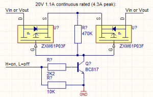
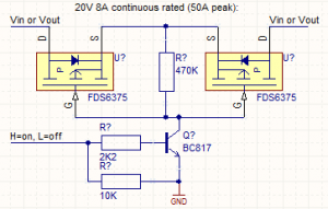
Using this back to back arrangement of P Channel mosfets, when on current will flow in either direction. When off both sides are isolated. You can use any typical P channel mosfet.


The transistor switch is needed because the gates need to be switched by an open drain output to avoid there being a large enough Vgs from the on off signal in relation to the power rails connected to the Drains being switched . The transistor could be lost of an open drain IC which can tolerate the Drain voltages when off is used to provide the signal.
Note that this arrangement is only suitable if the voltage being switched is > Vgs switching threshold of the mosfet used.
Where this can’t be guaranteed or where opto isolation is needed, photo mosfet solid state relays are a great solution. Examples:
Avago ASSR-1218 – 200mA, 60V rated. Will hapily switch low voltages like +3V3 without any voltage drop other than caused by its on state resistance (i.e. without the voltage drop of using a transistor output opto isolator).
Mosfet True Switch / Bi-Directional Switch With N-Channel MOSFETs
An example:

Why MOSFETs Fail
Insufficient gate drive
MOSFET devices are only capable of switching large amounts of power because they are designed to dissipate minimal power when they are turned on. You must ensure that the MOSFET is turned hard on to minimise dissipation during conduction. If the device is not fully turned on then the device will have a high resistance during conduction and will dissipate considerable power as heat.
Over Voltage
Exceed a MOSFETs voltage rating for just a few nS and you can destroy it. Select MOSFET devices conservatively for the anticipated voltage levels and ensure you allow for or deal with suppressing any voltage spikes or ringing.
Peak current overload
Overload currents for a short duration can cause progressive damage to a MOSFET often with little noticeable temperature rise prior to failure. MOSFETS often quote high peak current rating but these are typically only for peak currents of a few 100 uS. If switching inductive load ensure you overrate the MOSFET to handle peak currents.
Prolonged current overload
If a MOSFET is passing a high current then its on state resistance will cause it to heat up. If the heatsinking is poor then the MOSFET can be destroyed by excessive temperature. A solution to this can be to parallel multiple MOSFETs to share high load currents between them.
H or Full Bridge Configuration Shoot-through / Cross conduction
When using P and N MOSFETS between voltage rails to provide a H or L output voltage, if the control signals to the MOSFETs overlap then they will effectively short circuit the supply and this is known as a shoot-through condition. When it occurs any supply decoupling capacitors are discharged rapidly through both devices every time a switching transition occurs and resulting in very short but large current pulses.
To avoid this you must allowing a dead time between switching transitions, during which neither MOSFET is turned on.
No free-wheel current path
When switching inductive loads there must be a path for back EMF to free-wheel when the MOSFET switches off. Enhancement mode MOSFETs incorporate a diode that provides this protection.
Slow reverse recovery of MOSFET body diode
High Q resonant circuits are capable of storing considerable energy in their inductance and self capacitance. Under certain tuning conditions, this causes the current to “free-wheel” through the internal body diodes of the MOSFET devices as one MOSFET turns off and the other device turns on. A problem arises due to the slow turn-off (or reverse recovery) of the internal body diode when the opposing MOSFET tries to turn on. MOSFET body diodes generally have a long reverse recovery time compared to the performance of the MOSFET itself. If the body diode of one MOSFET is conducting when the opposing device is switched on, then a “short circuit” occurs similar to the shoot-through condition described above. You can solve his problem by adding a Schottky diode connected in series with the MOSFET source (prevents the MOSFET body diode from ever being forward biased by the free-wheeling current) and a high speed (fast recovery) diode connected in parallel to the MOSFET/Schottky pair so that the free-wheeling current bypasses the MOSFET and Schottky completely. This ensures that the MOSFET body diode is never driven into conduction. The free-wheel current is handled by the fast recovery diodes which present less of a shoot through problem.
Excessive gate drive
If the MOSFET gate is driven with too high a voltage the gate oxide insulation can be punctured effectively destroying the MOSFET. Ensure that the gate drive signal is free from any narrow voltage spikes that could exceed the maximum allowable gate voltage.
Slow switching transitions
Little energy is dissipated during the steady on and off states, but considerable energy is dissipated during the times of a transition. Therefore it is desirable to switch between states as quickly as possible to minimise power dissipation during switching. Since the MOSFET gate appears capacitive, it requires considerable current pulses in order to charge and discharge the gate in a few tens of nano-seconds. Peak gate currents can be as high as an amp.
Spurious oscillation
MOSFET inputs are relatively high impedance, which can lead to stability problems. Under certain conditions high voltage MOSFET devices can oscillate at very high frequencies due to stray inductance and capacitance in the surrounding circuit. (Frequencies usually in the low MHz.) A low impedance gate-drive circuit should also be used to prevent stray signals from coupling to the gate of the device.
Conducted interference with controller
Rapid switching of large currents can cause voltage dips and transient spikes on the power supply rails which may interference with the control circuitry. Good decoupling and star-point grounding techniques should be used.
Static electricity damage
MOSFETs are very sensitive to static. Antistatic handling precautions should be used to prevent gate oxide damage.
Other Mosfet Resources
http://robots.freehostia.com/SpeedControl/Mosfets.html


Pingback: PIC/MOSFET PWM Model Train Controller | SusaNET
11 years ago
Hi Rick,
The same thing: it makes a near perfect switch. Even better than using P-MOSFETs. But the gate voltage has to be driven relative to the source. So if you use an N-MOSFET switch to switch 24V, you need like 36V to drive the gates of the FETs. Like the P-FET needs a drive 12 Volts below the 24V. But that is easy to make.
Normally you would use P-FET switches to switch the plus and you would use N-FET switches to switch the minus.
Since N-FETs are “better” than P-FETs some take the effort to use N-FETs and make a special gate drive charge pump. There are “high side drivers” that have this charge pump internally.
11 years ago
Great, very good point on – ‘Slow reverse recovery of MOSFET body diode’. Thanks.
10 years ago
Hi,
Good article. Thank you.
I’ve just sent out into the world a circuit with a back to back P – channel mosfet switch where the body diodes facing away from each other (the two sources are connected together). Are there any disadvantages to this?
thanks again,
Mike
9 years ago
what hapens if the gate current changes .. what is the effect on the channel current
4 years ago
@Madiha I will just reply 4 years later for anyone else
Mosfets don’t take almost any current via gate. Only a small amount during the switch, to charge the gate as if it were a capacitor.
How “hard” they turn on depends on the voltage of the base relative to source (for N-channel, rise gate above source to turn on, for P-channel, pull gate below source to turn on)
How “hard” they turn on dictates their resistance, and that dictates current based on ohms law. But you usually don’t want to work in mosfets in “non-saturated” mode where they have significant resistance compared to fully turned on.